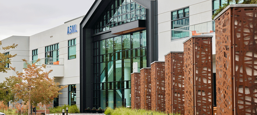
ASML has welcomed employees, local public officials and the media to the opening celebration of its new campus in Silicon Valley, California. The 212,573 square-foot facility includes a Class 1000 cleanroom, lab space and collaboration areas to advance ASML’s holistic lithography portfolio – hardware, software and services used to generate circuit patterns on silicon in high-volume production of microchips.
It’s no longer enough to address the various semiconductor manufacturing steps in isolation. The Silicon Valley team co-optimises IC designs, photomasks, lithography and metrology and inspection to enhance manufacturability and yield of leading-edge semiconductors through its expertise in computational lithography and e-beam metrology and inspection.
“As chipmakers continue to shrink the patterns to make small and powerful chips, we continue to grow to address the escalating complexities that require ever-more sophisticated approaches,” said Jim Koonmen, Executive Vice President of Applications Business at ASML. “It would be impossible to manufacture at dimensions of 10nm or smaller without our software and metrology solutions, and we have a long-term roadmap to help our customers overcome their future chip production challenges.”
ASML first established its presence in Silicon Valley 20 years ago and now more than 875 employees work at the new campus. In addition, the team plans to grow 20% in 2022, hiring more than 180 engineers to execute its product roadmap and meet the insatiable demand for more microchips.
Click below to share this article